





Researchers in China have developed a sensor that could reduce the amount of energy that drones and other autonomous hardware use to process visual data.
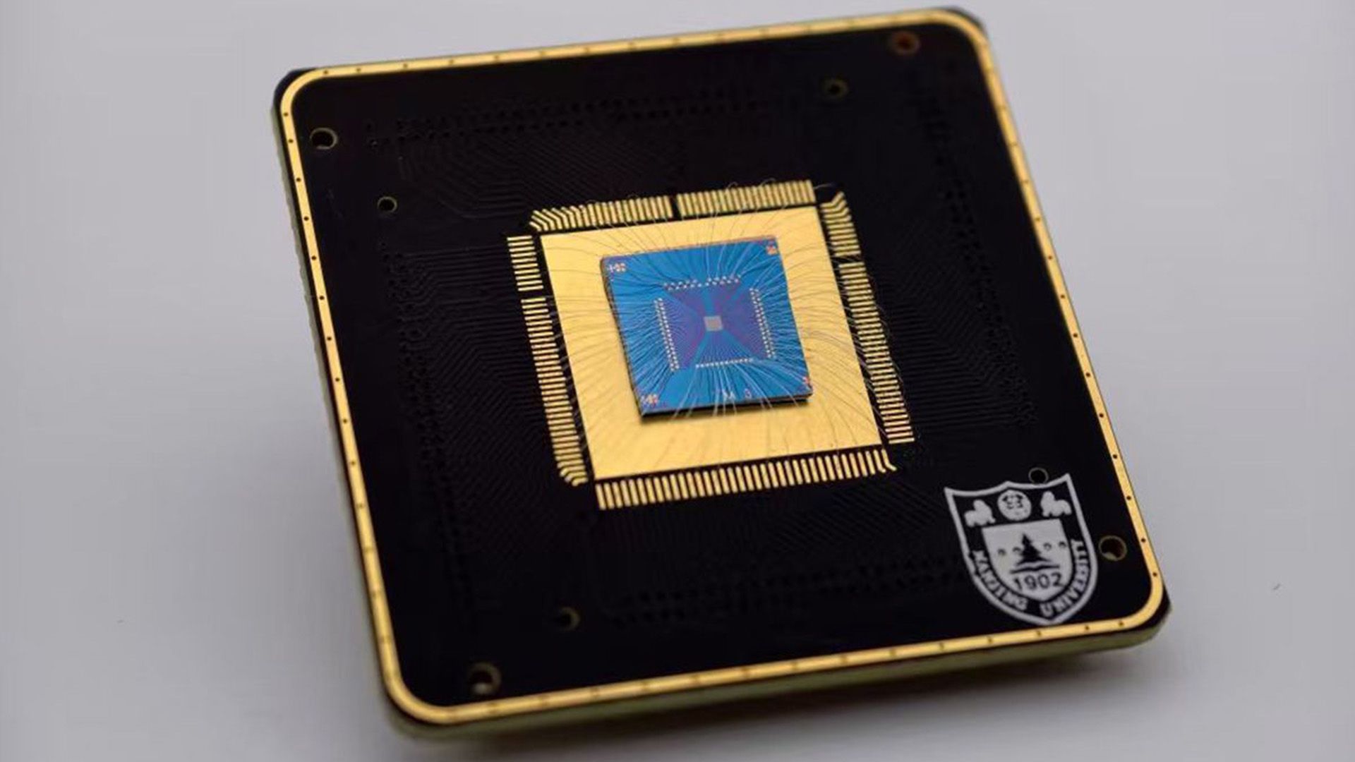
In a study published Aug. 19 in the journal Nature Sensors, scientists detailed the architecture of a new 2D chip dubbed “LightTok,” which can convert raw light into tokens used by artificial intelligence (AI) models on the chip itself. The device skips several energy-intensive steps that conventional sensor systems depend on, the scientists said.
“Our design idea was to move token generation onto the sensor itself, allowing the chip to directly produce tokens that AI models can process once light reaches the sensor,” Miao Feng, director of Nanjing University’s Institute of Brain-Inspired Intelligence, said in a statement. “These tokens contain complete image information.”
Latest Videos FromLive Science
Collapsing the visual perception process
In conventional visual perception, light signals have to go through multiple stages. A sensor captures the signals, and an analog-to-digital converter turns the light into pixels. That data is then stored temporarily before it’s shuttled to a separate chip, where the image is cut into square “compartments” — much like dividing a photo into a grid of tiles. Each compartment is then converted into a token for an AI model to read.
One study widely cited by other academics found that an analog-to-digital converter is responsible for 66% of an image sensor’s energy consumption, on average. Moving visual data processing off the chip and into the cloud can increase overall energy consumption further.
LightTok’s solution to the energy problem is to collapse the five stages into one by building the sensing, memory and computation processes into the same pixel. The researchers achieved this through an array based on a technology called a single-layer molybdenum disulfide floating-gate phototransistor that can sense light, remember what it sensed, and then factor that into a calculation.
The chip physically eliminates data movement, which is the main source of energy waste.
Liang Shi-Jun, physics professor at Nanjing University
Molybdenum disulfide is a 2D material that reacts well to light and can be grown in sheets one atom thick. The phototransistor converts incoming photons — particles of light — into an electrical current, while the floating gate is an isolated component inside the phototransistor that can trap and hold an electrical charge, rather than disappearing after the light goes away.
Get the world’s most fascinating discoveries delivered straight to your inbox.
Liang Shi-Jun, a physics professor at Nanjing University, summarized the chip to Chinese state-run news agency Xinhua. “The chip physically eliminates data movement, which is the main source of energy waste,” Liang said. “Light comes in, tokens come out” — hence the name “LightTok.”
LightTok achieved 87.3% accuracy in image recognition during tests — compared to the conventional, multi-step process described above —- while being 10 times more energy efficient at converting light into tokens, the researchers reported in the study.
A more efficient physical world
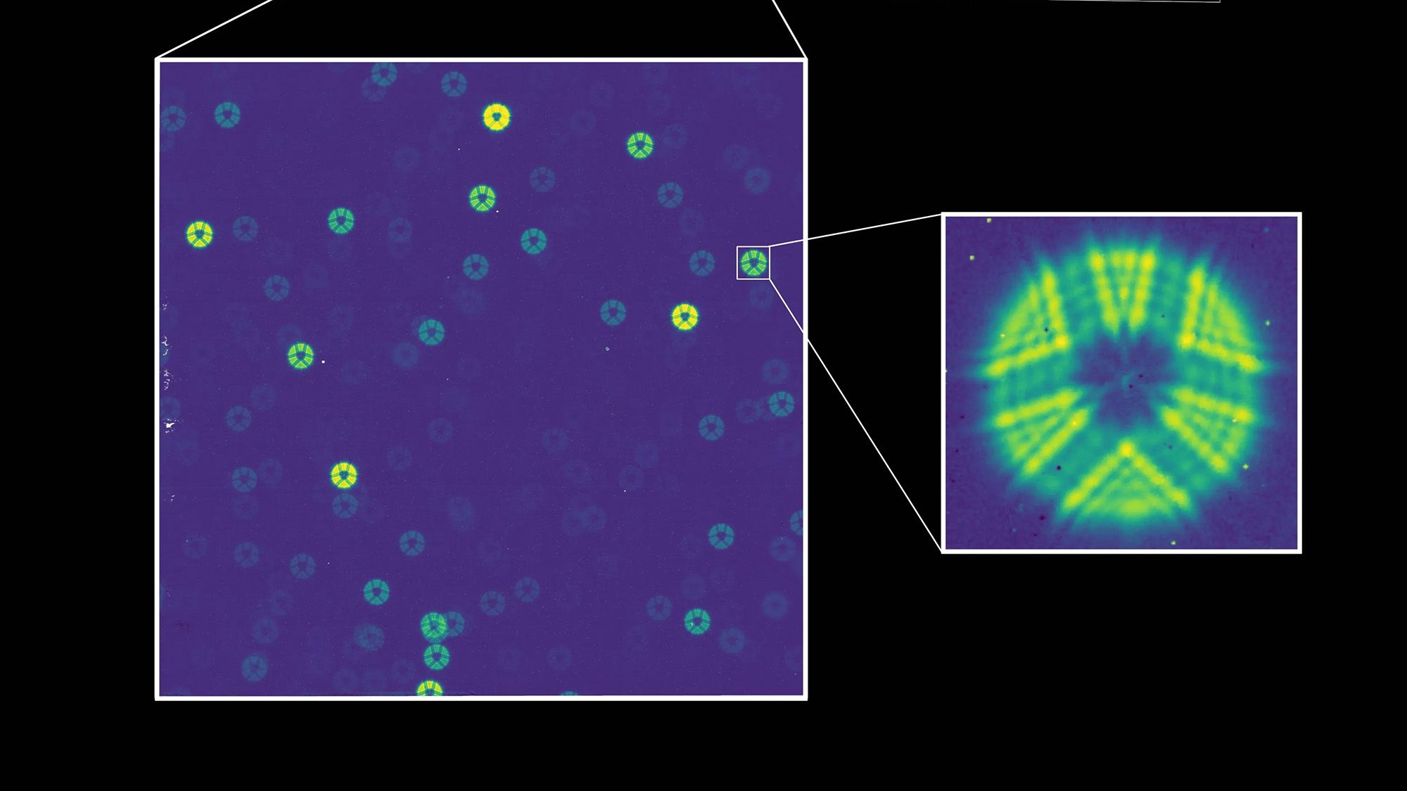
At present, LightTok’s maximum resolution is just 32 by 32 photosensitive pixels — the light-sensitive compartments on an image sensor that capture the visual data. This is far inferior to the quality of current smartphone cameras, let alone drones and autonomous hardware.
Nevertheless, Miao said in the statement that there’s an opportunity for the technology to be scaled up using the complementary metal-oxide-semiconductor manufacturing process — the same method used to fabricate chips found in smartphones and laptops as well as sensors in drones.
The researchers believe that if LightTok can eventually scale successfully, it could transform the operation of remote sensing technology. For example, a drone scanning a disaster zone or remote area could potentially fly longer because less energy is required for visual processing.
Kumar Sokka, CEO of Acre Security, a company that provides real-world sensing for critical infrastructure, described the work as a “small-scale demonstration.” However, “the direction [of the research] matters to anyone working in the physical world,” added Sokka, who was not involved in the new research.
Sokka, who previously spent 15 years at industrial automation company Rockwell Automation, told Live Science in an email that too much of the conversation around physical AI has centered around AI models. In truth, the bigger challenge has been the energy cost of “getting what a sensor sees into a form a model can actually use, right where the sensing happens,” he said.
The massive amount of energy typically required to turn raw data, such as light, into tokens “is wasteful when you’re running perception on a robot or an edge device with a tight power budget,” Sokka noted. However, processing at the point of detection may be “an enabler for pervasive physical AI, and a clever one, but it’s not a cure for the whole problem,” he added.
Can you match these ancient devices to their pictures? Find out with our computing quiz!